


Advanced Foundry Capabilities Through MOSIS 2.0
USC-led semiconductor prototyping initiative MOSIS 2.0 will be the official storefront for cutting-edge foundry services from domestic microelectronics leaders.
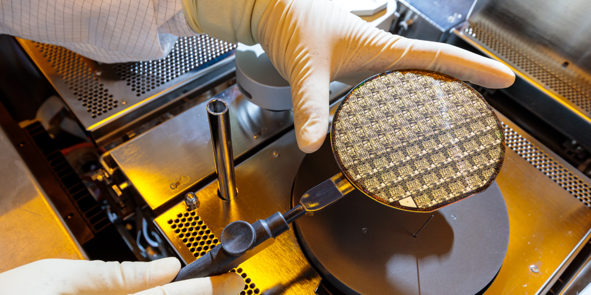
A semiconductor wafer. Image: Northrop Grumman
Three leading domestic microelectronics facilities, HRL Laboratories, Teledyne, and Northrop Grumman Microelectronics Center, are making their specialized foundry and advanced packaging capabilities accessible through the MOSIS 2.0 platform, offering unprecedented access to cutting-edge compound semiconductor and heterogeneous integration technologies. Each organization brings decades of heritage in defense and aerospace applications, operating as DoW-trusted foundries with proven track records in developing and manufacturing high-performance devices for the most demanding applications.
- HRL Laboratories, jointly owned by Boeing and GM, specializes in high-frequency GaN MMIC technology with their T3L process offering industry-leading performance through W-band frequencies.
- Teledyne Scientific Company, operating from their Thousand Oaks facility and formerly the Rockwell Science Center, provides world-class indium phosphide (InP) HBT technologies at 250nm and 130nm nodes for millimeter-wave applications exceeding 300 GHz, along with emerging GaN HEMT capabilities and 3D heterogeneous integration through their SLIC process.
- Northrop Grumman Microelectronics Center operates a comprehensive three-facility network spanning California, Maryland, and Florida, offering complete end-to-end solutions from compound semiconductor fabrication in GaAs, GaN, and InP through advanced 300mm wafer bumping and sophisticated packaging with interconnects down to 5-micron pitch.
Together, these facilities represent the domestic capability to design, fabricate, package, and test the most advanced RF and millimeter-wave systems, with flexible access models ranging from multi-project wafer runs and dedicated production to custom process development and lab-to-fab technology transfers, all available through commercial terms while maintaining rigorous IP protection and security protocols required for sensitive applications.
HRL Laboratories' GaN MMIC Foundry Capabilities and Offerings
David Fanning, representing HRL Laboratories' microfabrication operations, highlights their high-frequency GaN foundry node available through MOSIS 2.0. HRL is jointly owned by Boeing and GM, functioning as their advanced R&D laboratory with a mission to strengthen both LLC members and serve government and commercial customers. With heritage dating back to 1948 as the Hughes R&D Lab, HRL boasts an impressive innovation record of over 1,800 patents in the past twenty years and has been a DoW TAPO Trusted Foundry since 2008.
HRL is organized into four laboratories and one center, with the Microfabrication Technology Lab (MTL) serving as the cleanroom organization where specialty wafer processing and integration occurs. MTL operates a vertically integrated wafer fab with over 10,000 square feet of Class 10 cleanroom space plus an additional 6,000 square feet of Class 1000 space, with ISO and AS9100 certifications. The facility handles everything from epitaxial growth through die singulation, advanced fabrication, packaging, and testing, including capabilities for processing as a DoW-trusted foundry.
HRL has established four cross-laboratory thrust areas aimed at transitioning laboratory technologies into real-world applications, with GaN-based RF electronics being particularly relevant to their foundry offerings. The organization's GaN MMIC technology has evolved significantly since 2006, progressing from T2 GaN through T3 to their current T3L technology.
HRL has offered open access MPW services since 2019, marking the first sub-100-nanometer node GaN foundry to do so. The facility runs approximately four MPW cycles per year, serving a diverse customer base including commercial, DoW, and DoW contractors both domestic and foreign. Access requires completing end-user statements and security procedures. This platform ensures secure transmission and storage of customer IP with appropriate cyber certifications and firewalls between customers.
Foundry Processes:
- 40nm T3L GaN MPW and dedicated vehicle service
- N-polar GaN advanced node early access
- Custom flows
- InP HBT
- Infrared Focal Plane Arrays (IR FPAs)
- Si/SiGe Quantum Dot Qubits
- Magneto-sensors
- Contract R&D for compound semiconductors
Foundry Services:
- DoD / TAPO Trusted Foundry
- Electron beam lithography
- High frequency RF test
- Advanced packaging
Teledyne Scientific: High-Frequency Millimeter Wave Chips, Advanced GaN Power Amplifiers, and 3D Chip Integration Available for Multi-Project Wafer Runs
Teledyne Technologies is a $6 billion revenue organization serving high-end markets including defense, aerospace, and test and measurement sectors, with significant investments in semiconductor foundry capabilities across multiple facilities. They are partnering with MOSIS 2.0.
Teledyne Scientific, located in Thousand Oaks, California, operates a compound semiconductor and MEMS foundry with approximately 8,000 square feet of cleanroom space, specializing in early-stage R&D, prototyping, and low-volume production. Formerly the Rockwell Science Center, the facility has extensive heritage in compound semiconductor and MEMS technology development. The facility primarily operates at 100 millimeter wafer diameters but can accommodate both smaller and larger wafer sizes, which is particularly valuable for emerging compound semiconductor technologies where large substrates may not be readily available.
The foundry's operations encompass three core elements. First, traditional government-sponsored contract R&D with agencies like DARPA, focusing on advanced compound semiconductor devices, MEMS, and heterogeneous integration. Second, IC foundry processes and products that evolved from government-sponsored programs, including several lab-to-fab transitions from university partners. Those IC products are developed for the commercial market and tend to be focused on high-end applications, so test and measurement, where volumes are not necessarily large. To keep the fab level up, they engage in clean room fabrication services and prototyping for external customers who lack their own facilities.
Under the ME Commons program, they are acting as a core facility with a diverse toolset supporting a range of processes and materials, doing most of their work in the fab with 100-millimeter diameters, but they do have the capability to run both smaller and larger wafer sizes.
Indium Phosphide HBT Technologies:
- 250nm node: Production-ready, available for MPW runs
- 130nm node: Engineering development stage
- Designed for millimeter-wave applications
- Four-level back-end interconnects with gold metallization and BCB interlayer dielectrics
- Record performance in power amplifiers
Additional Foundry Processes:
- Low-noise indium phosphide HEMT process
- High-performance GaN HEMT process (in development)
- Silicon RF interposer process for millimeter-wave phased array applications
GaN Charge HEMT Technology (Under Development):
- Low on-resistance and high current density
- Minimal DC-to-RF dispersion effects
- Linear compression characteristics without soft gain compression
- Good scalability of output power with quiescent bias
SLIC 3D Heterogeneous Integration:
- Silicon interposer-based process with etched recesses
- Enables integration of different die types
- IC-grade interconnects on planarized surface
- Through-substrate vias for board attachment
- Four-level interconnect process
- Not currently offered for MPW (requires coordination with users)
Beyond foundry processes, Teledyne provides flexible fabrication and prototyping services ranging from simple process modules to complete process transfers from university nanofabs, including low-volume pilot production. These services support diverse technologies, including GaN micro-LEDs, infrared detectors, MEMS devices, and silicon photonics, all delivered on fixed-price terms with comprehensive engineering support from experienced staff.
Northrop Grumman Microelectronics Center: Complete Compound Semiconductor Foundry Services from Design to Production
Northrop Grumman's Microelectronics Center (NGMC) is a purpose-built organization designed to provide flexible, assured microelectronics capabilities for commercial companies, government agencies, and defense industrial base partners. The center operates three facilities: the Advanced Technology Laboratory in Baltimore, Maryland, a foundry in Redondo Beach, California focused on compound semiconductors, and an advanced packaging facility in Central Florida. All facilities are DMEA-trusted suppliers with AS9100 certification.
Access to NGMC capabilities is primarily through their Microelectronics Products and Services (MPS) organization, which has served as their commercial storefront for over twenty years.
MPS offers fixed-price contracts with commercial terms, providing everything from design services and foundry runs to multi-project wafer runs, post-processing, and complete RF unit delivery. Customers can also access these services through MOSIS 2.0, which connects directly to MPS. The organization emphasizes that working with MPS is distinctly different from traditional Northrop Grumman partnerships, operating as a true commercial contract relationship.
The compound semiconductor foundry at Space Park, California, offers comprehensive capabilities in gallium arsenide (GaAs), gallium nitride (GaN), and indium phosphide. These technologies support RF, mixed-signal, and digital applications in GaAs; very high-power capabilities in GaN; and the highest frequency applications extending into terahertz ranges with indium phosphide. Each technology platform includes very mature nodes proven in space and DoW production, as well as commercial applications, alongside advanced pre-production nodes available for specific customer designs. The facility also features two chip-scale advanced packaging technologies: wafer-scale packaging that creates hermetically sealed packages with balls for flip-chip assembly, and DAHI technology for 3D heterogeneous integration.
The Advanced Technology Laboratory in Baltimore houses an exceptionally wide range of technologies under one roof. Capabilities include heritage silicon technologies operating at quarter-micron nodes, silicon carbide power technologies, heritage GaAs processes, and GaN SLCFET technology developed for high-performance switching applications. The facility also operates one of the world's largest superconducting fabrication capabilities and ultra-wide bandgap semiconductor technologies. All these technologies were originally developed for demanding DoW applications requiring exquisite performance and very high reliability.
NGMC's advanced packaging capabilities, developed over the past decade, address the domestic shortage of scalable advanced packaging from prototype through millions of units annually. Their Central Florida wafer post-processing facility offers highly flexible, scalable manufacturing across broad wafer sizes with particular emphasis on 300mm wafer bumping capabilities currently being expanded. The facility handles wafer sizes down to 100mm for compound semiconductors, offering various interconnect options including lead and lead-free solders, and copper pillars. Critical capabilities include automated optical inspection screening every bump on every wafer, production-level testing for known good die delivery, and development of advanced interconnects targeting UCIE specifications.
Assembly capabilities span both coasts, primarily concentrated in Baltimore, supporting standard flip-chip and mass reflow processing as well as thermocompression bonding for very small interconnects down to approximately 5-micron pitch. These parts can be assembled on substrates ranging from single organic chip-level interposers to wafer or panel scale, depending on volume requirements. A unique capability is their silicon carbide interposer technology from the West Coast facility, providing high reliability and thermal conductivity for heat extraction from high-performance devices.
Comprehensive test capabilities extend across the entire packaging stream, from individual device testing for RFICs, ASICs, and MMICs to package-level testing in automated handlers. These capabilities span digital through W-band and beyond frequencies, include classified testing for DoW applications, and encompass design services plus environmental and reliability testing. The emphasis is on complex mission applications requiring testing that typical foundries cannot or will not perform.
GaN HEMT Technologies:
- 150nm and 200nm nodes: In production, available for MPW runs
- Production-ready in January 2026
- Designed for high linearity and efficiencies at frequencies
- Available packaging options include Wafer Level Packaging, Cu-pillar, and Solder Bump
InP HEMT Technologies:
- 100nm node: In production, available for MPW runs
- Highest speed transistor in the world
- Broad-band LNAs with extremely low DC power consumption
Post Processing:
- Bumping Process includes passivation, under bump metal, electroplating, solder sphere drop process.
- Whole Wafer probing 150mm to 300mm wafer sizes
- Dicing process includes: A dice before grind mechanical saw, thinning, laser die marking, die sort into waffle packs and tape & reel
- Metrology processing including whole wafer bump shear, 100% 2D/3D bump measurements as well as process controls in place for passivation and UBM layers
- Wafer sizes capability: 100mm, 150mm, 200mm and 300mm
Advanced Assembly:
- Multi-die, multi-foundry flip-chip 2D/3D assembly
- High-accuracy thermocompression bonding
- Automated optical and x-ray inspections
- Organic, glass, silicon, and silicon carbide substrate handling
- Automated reflow, underfill, cleaning, ball attach
- High accuracy depaneling (mechanical, laser, saw)
- Hermetic wafer-level packaging
Distribution Statement A: Approved for public release. Distribution is unlimited.