About Us
The Legacy of MOSIS:
Four Decades of Innovation
-
1981: MOSIS Service Launch
USC's Information Sciences Institute introduces MOSIS, revolutionizing semiconductor access. DARPA funding enables the pioneering Multi-Project Wafer model.
-
1990s-2000s
MOSIS processes over 60,000 designs globally. Services extend to government labs, corporations, and universities worldwide.
-
2010s: Technological Advancements
MOSIS offers cutting-edge processes including CMOS FinFET, FD-SOl, and III-V Compound semiconductors. Educational outreach programs flourish.
-
2023: MOSIS 2.0 Launch
Includes MPW access to commercial foundries AND direct access to all major Southern California Academic Nanofabrication Facilities.
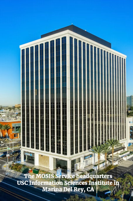
The University of Southern California’s Information Sciences Institute “ISI”, an organized research unit within the Viterbi School of Engineering received a series of contracts from DARPA beginning in 1981 to provide Integrated Circuit (IC) fabrication services for the US Government, primarily DARPA. ISI did pioneering work with developing what will become known as multi project wafer (MPW) capabilities. By June 1985, 1706 designs had been fabricated over the prior twelve months. In 1985, a joint DARPA and NSF program was initiated to provide VLSI fabrication access to Universities teaching VLSI design courses. In the fall of 1987, DARPA requested USC/ISI establish a commercial service so that USC could accept design fabrication orders from 3rd parties, which were expected to be primarily US Government contractors and Universities. USC did establish The MOSIS Service as a silicon prototyping and low volume production service for custom and semicustom ICs. MOSIS was an acronym of Metal Oxide Silicon Implementation System. They accepted customer designs in CIF, CALMA GDSII or MEBES format and delivered packaged parts. They were working with 13 mask fabrication houses and 7 different foundries in 1987. In addition to MPW services, MOSIS had a major focus providing wafer level reliability testing services to the design community.
MOSIS was one of the earliest and successful implementations of electronic commerce via the Internet (pre WWW) receiving designs via electronic mail and then providing access via the “Web” and “MOSAIC” commencing in 1993.
In the almost 40 years of service, The MOSIS Service has had over 50 US Government laboratories and agencies, 800 domestic and foreign colleges and Universities, and over 100 commercial companies submit designs for fabrication.
The University of Southern California through The MOSIS Service is committed to providing value add services to the microelectronics community into the future.
In 2023, MOSIS evolved into MOSIS 2.0 as a core component of the Defense Ready Electronics and Microdevices Superhub (CA DREAMS), one of eight regional innovation hubs established under the Department of War Microelectronics Commons Program through the CHIPS and Science Act of 2022. Building on our 40+ year legacy of providing Multi-Project Wafer (MPW) services, MOSIS 2.0 vastly expands its capabilities by offering comprehensive semiconductor prototyping solutions through an extensive network of partners, including seven university nanofabs, three DoW-volume fabs, and seven commercial foundries. Through a focus on standardization and unified process control measures the service can now provide access to over 350 tools and 35+ MPW supports, handling everything from "coupon-size" to 300mm wafers with features below 7nm. Through its Prototype Integration and Engineering Service (PIES) team, MOSIS 2.0 offers end-to-end support including rapid prototyping, design assistance, fabrication services, and testing, while serving three distinct customer segments: academic institutions, Department of War entities, and commercial companies. Lastly, the service maintains a strong focus on education, offering training programs, seminars, and workshops.