MOSIS 2.0 USC Viterbi Information Sciences Institute CA Dreams

Meet the Team

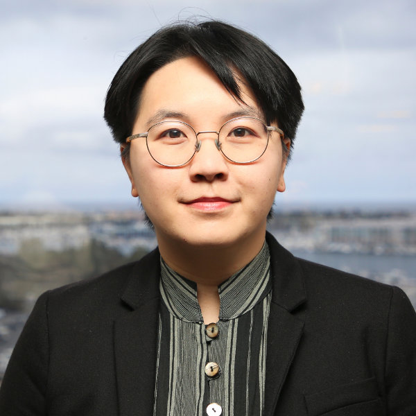
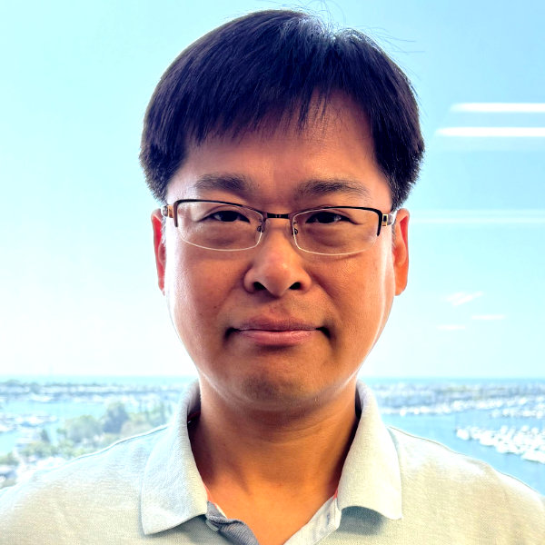
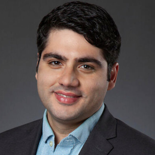
Mike Haney

Mike Haney

Deputy Director Director MOSIS 2.0

From 2014 to 2020, Michael Haney served as Program Director and later Program Director Emeritus at ARPA-E, while on assignment from the University of Delaware (UD), where he was a Professor of Electrical and Computer Engineering. At ARPA-E, he led transformative programs in high-efficiency solar energy and photonic networks for data centers. From 2006-2010, he was a Program Manager at DARPA’s Microsystems Technology Office, advancing integrated photonics for applications like bio-sensing and solar cells. In 1998, Haney co-founded Applied Photonics, Inc. to drive optical interconnect technology. He holds a Ph.D. from Caltech and degrees from Illinois and UMass Amherst.

Rehan Kapadia

Rehan Kapadia

Co-Director MOSIS 2.0

Professor Kapadia joined the University of Southern California's Ming Hsieh Department of Electrical Engineering in July 2014. He earned his bachelor’s degree in electrical engineering from the University of Texas at Austin in May 2008 and his Ph.D. from the University of California, Berkeley, in May 2013. While at Berkeley, he was a National Science Foundation Graduate Research Fellow and received the David J. Sakrison Memorial Prize for outstanding research. He has also won an AFOSR Young Investigator Award (2016), an ONR Young Investigator Award (2021), and the AVS Peter Mark Memorial Award (2020). His research focuses on next-generation electronic and photonic devices, material growth techniques, and the integration of compound semiconductors with arbitrary substrates, resulting in over 30 journal articles and multiple patents.

Christine Lee

Christine Lee

Fabrication Services Team Lead

Christine Lee is the Nanofab Process Improvement Team Lead for MOSIS 2.0. Before her role at MOSIS 2.0, she worked as a process engineer at Northrop Grumman, supporting the Space Park microelectronics foundry. Christine earned her M.S. in Materials Science & Engineering from UCLA and holds a B.S. in Materials Science from UC Berkeley. Her educational background and experience contribute to her expertise in enhancing nanofabrication processes and supporting advanced semiconductor manufacturing initiatives.

Damon McCaskill

Damon McCaskill

Senior Project Manager

Damon McCaskill serves as the Senior Project Manager for MOSIS 2.0, leveraging extensive project management experience evidenced by his PMP certification and a background as a former MMIC Design Engineer in the Aerospace/Defense industry. His expertise in guiding teams through complex projects and fostering collaboration makes him a vital asset to ISI. Before MOSIS 2.0, Damon contributed to high-impact projects at Hughes Space and Communications, Boeing Satellite Systems, Raytheon, and Mercury Defense Systems. He holds a B.S. in Electrical Engineering from Morgan State University and a Master's in Electrical Engineering from Cornell University.

Lifu Chang

Lifu Chang

Integrated Circuit Design Team Lead

Dr. Lifu Chang is the Director of Supply Chain at MOSIS 2.0, where he envisions it as a key provider of semiconductor manufacturing and yield enablement for advanced chip designs. With over 20 years of experience in semiconductor technology, Electronic Design Automation (EDA), and Design for Manufacturability (DFM), he has held leadership roles at companies like SMIC, Qualcomm, and Hisilicon. Dr. Chang pioneered DFM technology and led the development of critical processes for improving yield and optimizing advanced chip designs. Dr. Chang earned his Ph.D. from Purdue in 1996, holds multiple patents, published 50 papers, and is an IEEE Senior Member.

Jeung Hun Park

Jeung Hun Park

MPW Services Team Lead

Dr. Jeung Hun Park is a materials scientist and Senior Engineering Manager at MOSIS 2.0, specializing in material design, synthesis, characterization, and microfabrication. His expertise includes advanced in situ/operando imaging techniques in reactive environments, fostering innovation in information display technologies, energy materials, and semiconductor devices. Previously, he served as the Wafer Fabrication Department Manager at Illinois Tool Works. He earned his Ph.D. in Materials Science and Engineering from UCLA and has held key positions at Princeton University, MIT, Columbia University, IBM T.J. Watson Research Center, and Samsung Electronics, focusing on developing advanced imaging systems, information display, and semiconductor devices.